- English
- Español
- Português
- русский
- Français
- 日本語
- Deutsch
- tiếng Việt
- Italiano
- Nederlands
- ภาษาไทย
- Polski
- 한국어
- Svenska
- magyar
- Malay
- বাংলা ভাষার
- Dansk
- Suomi
- हिन्दी
- Pilipino
- Türkçe
- Gaeilge
- العربية
- Indonesia
- Norsk
- تمل
- český
- ελληνικά
- український
- Javanese
- فارسی
- தமிழ்
- తెలుగు
- नेपाली
- Burmese
- български
- ລາວ
- Latine
- Қазақша
- Euskal
- Azərbaycan
- Slovenský jazyk
- Македонски
- Lietuvos
- Eesti Keel
- Română
- Slovenski
- मराठी
- Srpski језик

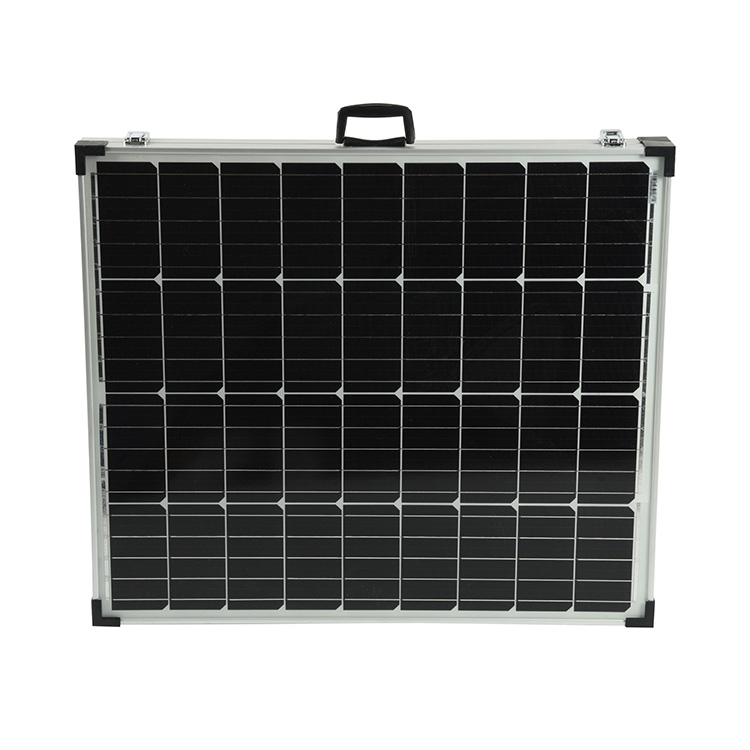
The manufacturing process of the solar panel(2)
2021-12-16
(5) Peripheral etching( solar panel): the diffusion layer formed on the peripheral surface of the silicon wafer during diffusion will short circuit the upper and lower electrodes of the battery. The peripheral diffusion layer shall be removed by masking wet etching or plasma dry etching.
(6) Remove the back PN + junction(solar panel). Wet etching or grinding method is commonly used to remove the back PN + junction.
(7) Making upper and lower electrodes(solar panel): vacuum evaporation, electroless nickel plating or aluminum paste printing and sintering are used. The lower electrode is made first, and then the upper electrode is made. Aluminum paste printing is a widely used process method.
(8) Making antireflection film(solar panel): in order to reduce the input reflection loss, a layer of antireflection film shall be covered on the surface of silicon wafer. The materials for making antireflection film include MgF2, SiO2, Al2O3, SiO, Si3N4, TiO2, Ta2O5, etc. the process methods can be vacuum coating method, ion coating method, sputtering method, printing method, PECVD method or spraying method.
(9) Sintering: the battery chip is sintered on the base plate of nickel or copper.
(10) Test classification: test classification according to the specified parameters and specifications.